
Growing adoption of silicon photonics in high-speed data communication, increasing demand for AI-driven data centers, and rising investments in advanced semiconductor testing are driving the growth of the silicon photonics test equipment market worldwide.
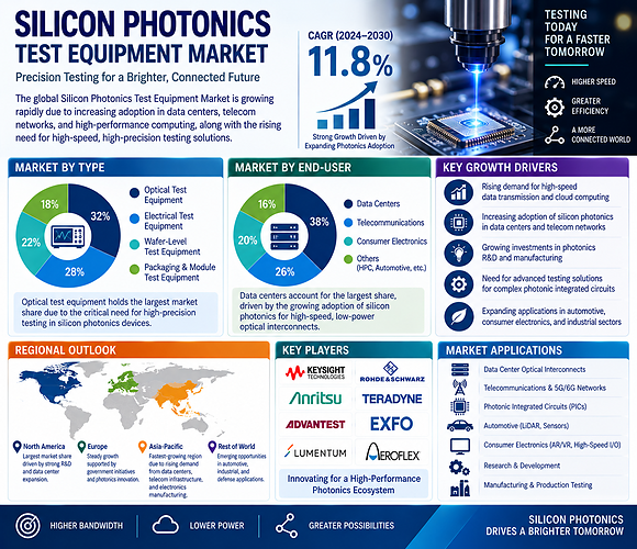
The global silicon photonics test equipment market is witnessing strong growth as semiconductor manufacturers, integrated device manufacturers (IDMs), foundries, and photonics companies increasingly invest in advanced testing solutions to ensure the performance, reliability, and yield of silicon photonic devices. Silicon photonics combines optical and electronic components on a single chip, enabling high-bandwidth, low-power data transmission for applications including data centers, telecommunications, high-performance computing, AI infrastructure, automotive sensing, and quantum technologies. Continuous advancements in wafer-level testing, automated optical alignment, high-speed measurement systems, and integrated photonic packaging continue to support market expansion. The market is projected to register a CAGR of 11.8% during the forecast period.
Key Growth Driver
Increasing deployment of silicon photonics for AI infrastructure and high-speed optical communication is accelerating market growth globally.
The rapid expansion of hyperscale data centers, cloud computing, 5G/6G network infrastructure, and artificial intelligence workloads is creating strong demand for high-performance silicon photonic devices. Manufacturers are investing in automated wafer probing, optical alignment systems, high-speed characterization platforms, and advanced reliability testing to improve manufacturing efficiency and reduce production costs while maintaining product quality.
Segment Highlight
Wafer probing systems and grating coupler test technologies continue to create significant growth opportunities.
Based on equipment type, Wafer Probing Systems (Electrical & Photonic) account for a significant share of the market owing to their ability to perform high-throughput wafer-level testing, early defect detection, yield optimization, and cost reduction. Optical Test & Measurement Systems continue to witness rapid growth as manufacturers require highly accurate optical characterization for next-generation photonic integrated circuits (PICs). Automated Test Equipment (ATE) Platforms, Die Handling & Test Automation Systems, Reliability & Burn-in Test Systems, Probe Cards & Optical Interface Assemblies, and other specialized equipment continue to support advanced semiconductor manufacturing.
By optical interface technology, Grating Coupler (Vertical Coupling) Test Systems dominate the market due to their widespread adoption in wafer-level testing, simplified optical alignment, and compatibility with high-volume silicon photonics manufacturing. Multi-channel / Parallel Test Systems are experiencing strong growth as manufacturers seek higher throughput and lower testing costs. Edge Coupling Test Systems, Free-space Optical Test Systems, Polarization-diverse Test Systems, and other advanced optical interface technologies continue to support specialized photonic testing applications.
Regional Opportunity
North America remains the leading market, while Asia-Pacific is emerging as the fastest-growing region for silicon photonics test equipment.
North America maintains a dominant position in the Silicon Photonics Test Equipment Market due to strong semiconductor research capabilities, increasing investments in AI infrastructure, presence of leading technology companies, and continuous innovation in photonic integrated circuits. Europe continues to witness significant growth supported by advanced semiconductor research programs, photonics innovation initiatives, and increasing adoption of high-speed optical communication technologies. Meanwhile, Asia-Pacific is expected to experience the fastest growth driven by expanding semiconductor manufacturing capacity, increasing investment in advanced packaging, growing production of photonic devices, government support for semiconductor self-sufficiency, and rapid expansion of data center infrastructure across China, Taiwan, Japan, South Korea, Singapore, and India.
Competitive Landscape
Market participants are focusing on high-speed optical measurement systems, automated wafer testing, precision optical alignment, and intelligent semiconductor test automation to strengthen their competitive position.
Leading companies are investing in AI-enabled testing platforms, precision motion control systems, high-bandwidth optical analyzers, automated die handling technologies, and advanced reliability testing solutions to improve throughput and measurement accuracy. Strategic collaborations with semiconductor manufacturers, foundries, photonics research institutes, and packaging companies continue to accelerate product innovation. Manufacturers are also emphasizing scalable testing platforms, reduced test time, high-volume manufacturing support, and compatibility with next-generation photonic integrated circuits.
Key companies operating in the market include Advantest Corporation, Aehr Test Systems, Anritsu Corporation, Cohu Inc., Enlitech Co., Ltd., EXFO Inc., ficonTEC Service GmbH, FormFactor Inc., Keysight Technologies, MPI Corporation, Nexus Test Pte. Ltd., Physik Instrumente (PI), Rohde & Schwarz, Semight Instruments, SemiProbe Inc., STAr Technologies, Teradyne Inc., VIAVI Solutions, and Yokogawa T&M.
Silicon Photonics Test Equipment Industry News
Jun 2026: Keysight Technologies expanded advanced photonic test solutions supporting high-speed optical device characterization for AI and data center applications.
Apr 2026: Advantest Corporation strengthened semiconductor test capabilities with continued investment in next-generation photonic testing platforms.
Jan 2026: FormFactor Inc. enhanced wafer probing technologies to support high-volume silicon photonics manufacturing and advanced packaging.
Oct 2025: VIAVI Solutions introduced expanded optical measurement solutions for photonic integrated circuit testing and network component validation.
Aug 2025: EXFO Inc. advanced optical testing technologies supporting high-performance silicon photonics development for telecommunications and cloud infrastructure.
Historical & Forecast Period
This study report represents analysis of each segment from 2024 to 2034 considering 2025 as the base year. Compounded Annual Growth Rate (CAGR) for each of the respective segments estimated for the forecast period of 2026 to 2034.
The current report comprises of quantitative market estimations for each micro market for every geographical region and qualitative market analysis such as micro and macro environment analysis, market trends, competitive intelligence, segment analysis, porters five force model, top winning strategies, top investment markets, emerging trends and technological analysis, case studies, strategic conclusions and recommendations and other key market insights.
Research Methodology
The complete research study was conducted in three phases, namely: secondary research, primary research, and expert panel review. key data point that enables the estimation of Silicon Photonics Test Equipment Market - Growth, Share, Opportunities & Competitive Analysis, 2026 - 2034 market are as follows:
Market forecast was performed through proprietary software that analyzes various qualitative and quantitative factors. Growth rate and CAGR were estimated through intensive secondary and primary research. Data triangulation across various data points provides accuracy across various analyzed market segments in the report. Application of both top down and bottom-up approach for validation of market estimation assures logical, methodical and mathematical consistency of the quantitative data.
| ATTRIBUTE | DETAILS |
|---|---|
| Research Period | 2024-2034 |
| Base Year | 2025 |
| Forecast Period | 2026-2034 |
| Historical Year | 2024 |
| Unit | USD Million |
| Segmentation | |
Test Insertion Type
|
|
Equipment Type
|
|
Optical Interface Technology
|
|
Application
|
|
End-user
|
|
|
Region Segment (2024-2034; US$ Million)
|
Frequently Asked Questions
Q1. What is driving the growth of the Silicon Photonics Test Equipment Market?
The market is primarily driven by increasing adoption of silicon photonics in AI infrastructure, expanding hyperscale data centers, rising demand for high-speed optical communication, and growing investment in advanced semiconductor manufacturing.
Q2. What is the expected growth rate of the Silicon Photonics Test Equipment Market?
The global Silicon Photonics Test Equipment Market is projected to expand at a CAGR of 11.8% during the forecast period.
Q3. Which equipment type accounts for a significant market share?
Wafer Probing Systems (Electrical & Photonic) account for a significant market share due to their ability to enable high-throughput wafer-level testing, improve manufacturing yield, and reduce production costs.
Q4. Which optical interface technology dominates the Silicon Photonics Test Equipment Market?
Grating Coupler (Vertical Coupling) Test Systems dominate the market owing to their efficient wafer-level optical coupling, simplified alignment, and suitability for high-volume silicon photonics production.
Q5. Which region is expected to witness the strongest market growth?
Asia-Pacific is expected to witness the strongest market growth due to expanding semiconductor fabrication capacity, increasing investments in photonic integrated circuits, rapid data center expansion, and strong government support for advanced semiconductor manufacturing.


